PCB Design View
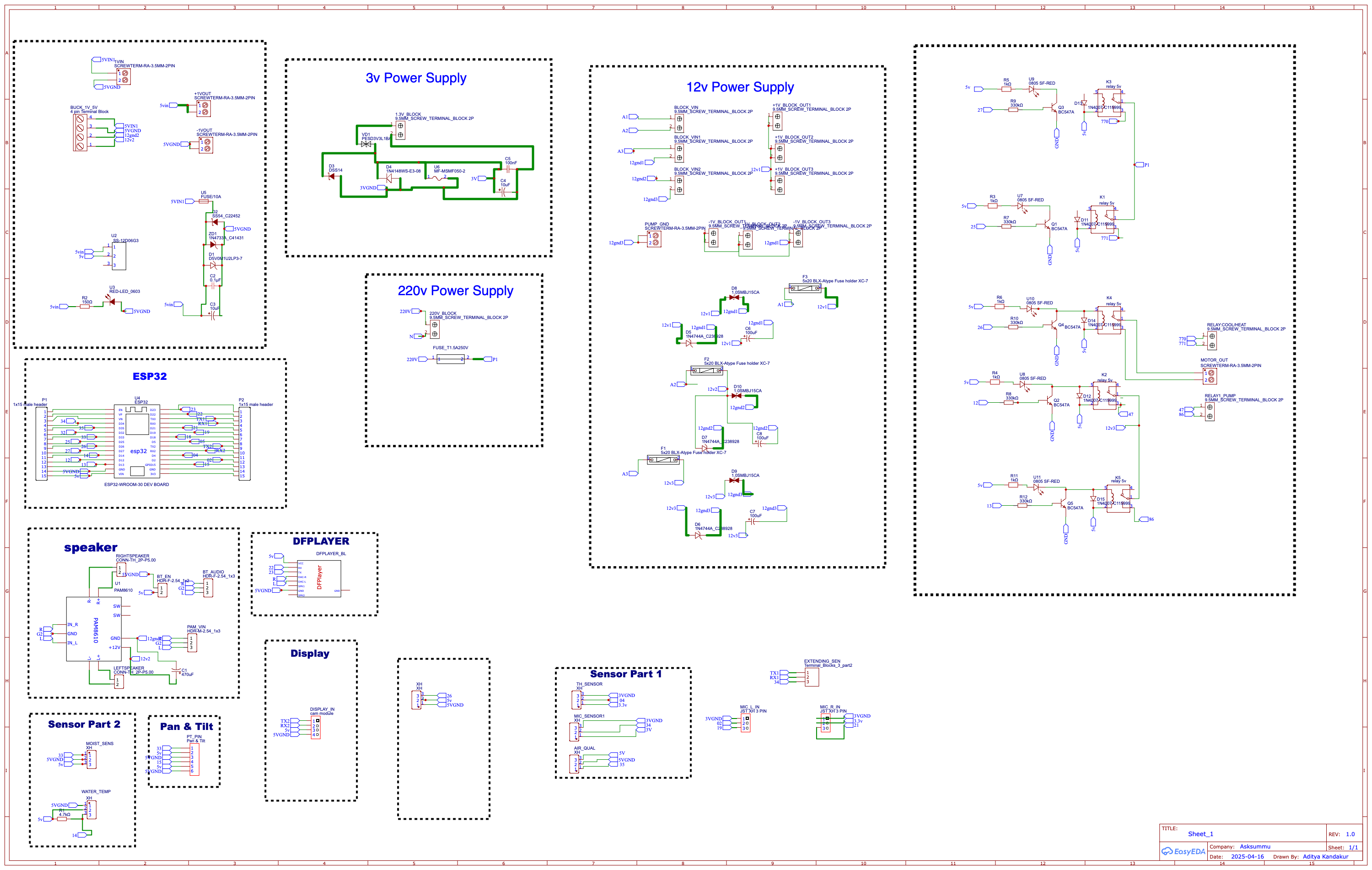
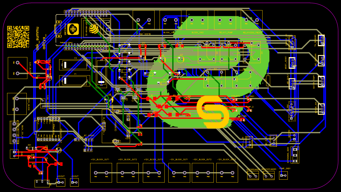
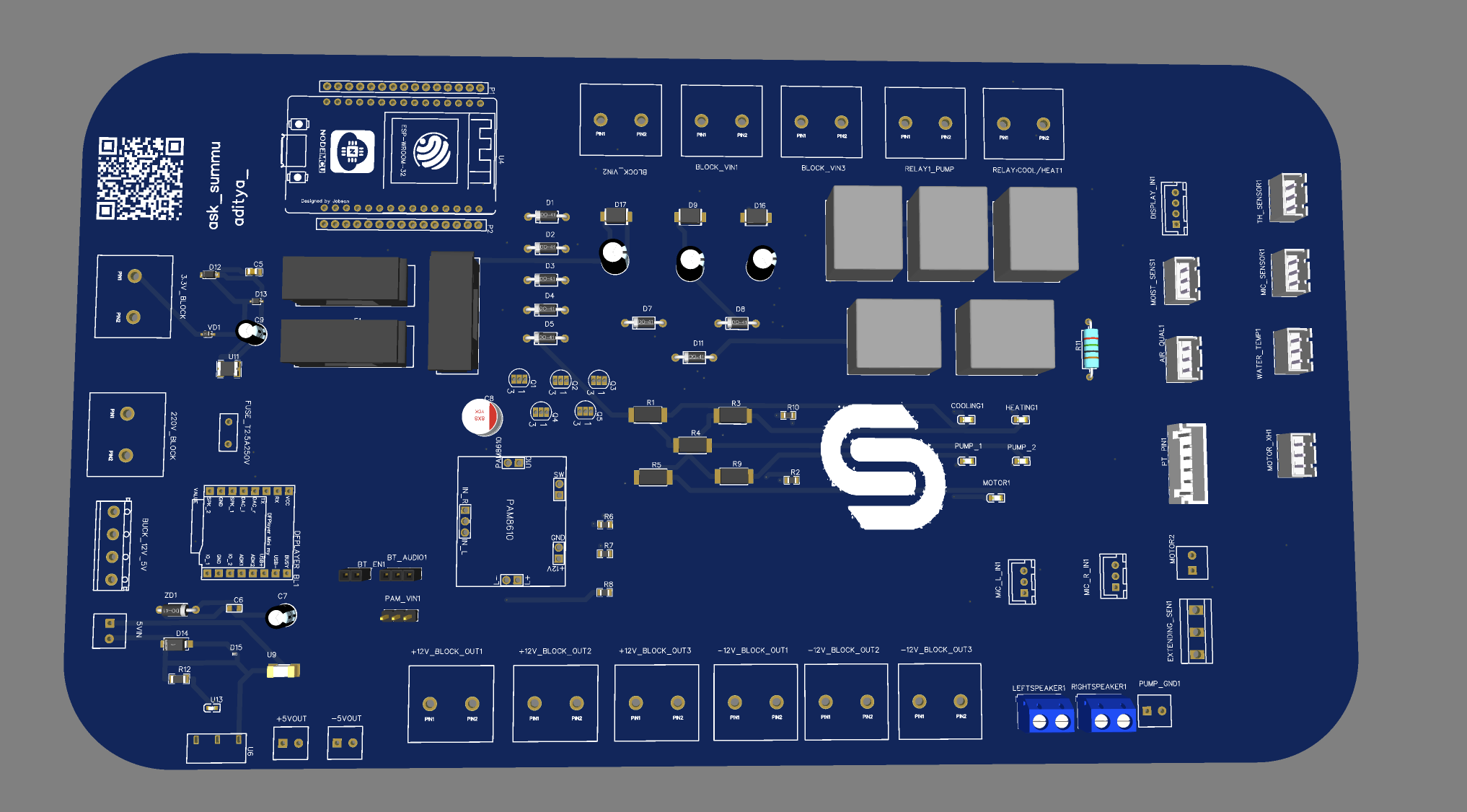
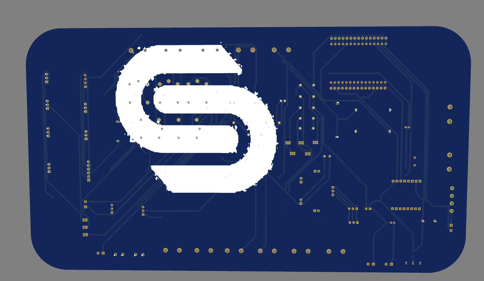
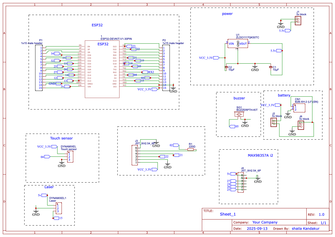
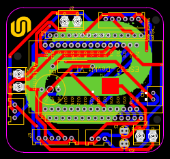
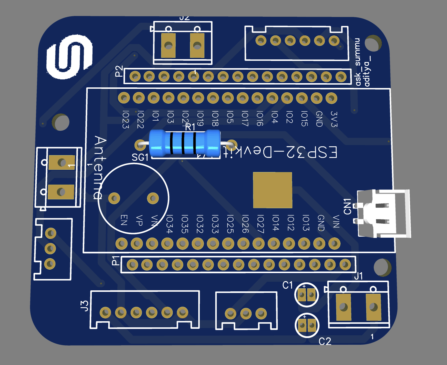
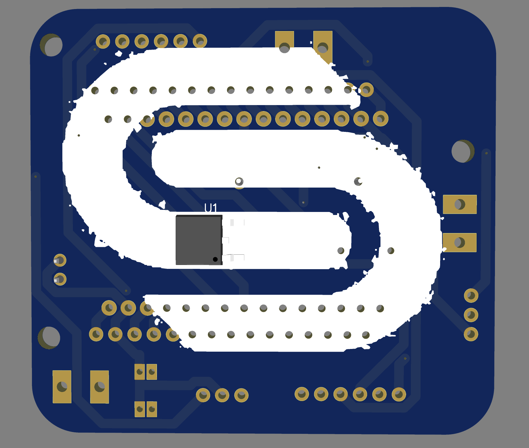
4-layer PCB for AI Baby Monitoring System
Advanced 4-layer main control board for the IntelliCradle AI baby monitoring system. Features dedicated power and ground planes for superior noise immunity, high-speed signal routing between ESP32 and multiple sensors, and optimized thermal management for continuous operation.
Design Achievement: Successfully transitioned from 2-layer to 4-layer design, achieving superior signal integrity and noise reduction for sensitive analog sensor circuits.
Click on any image to view in full-screen mode with zoom controls
2-layer capacitive touch interface PCB
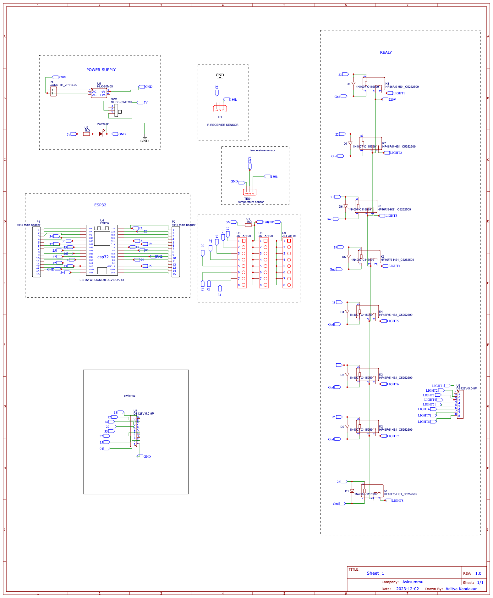
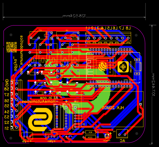
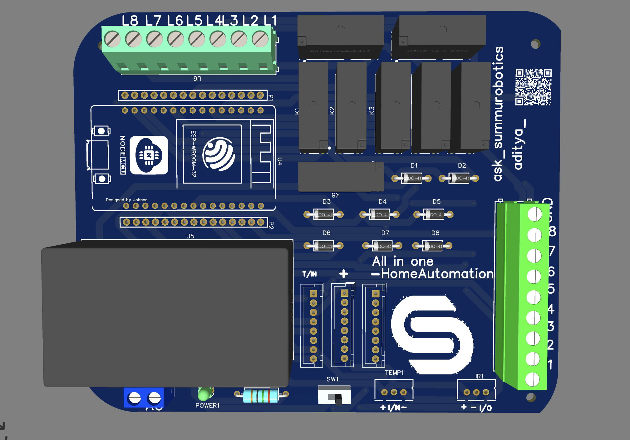
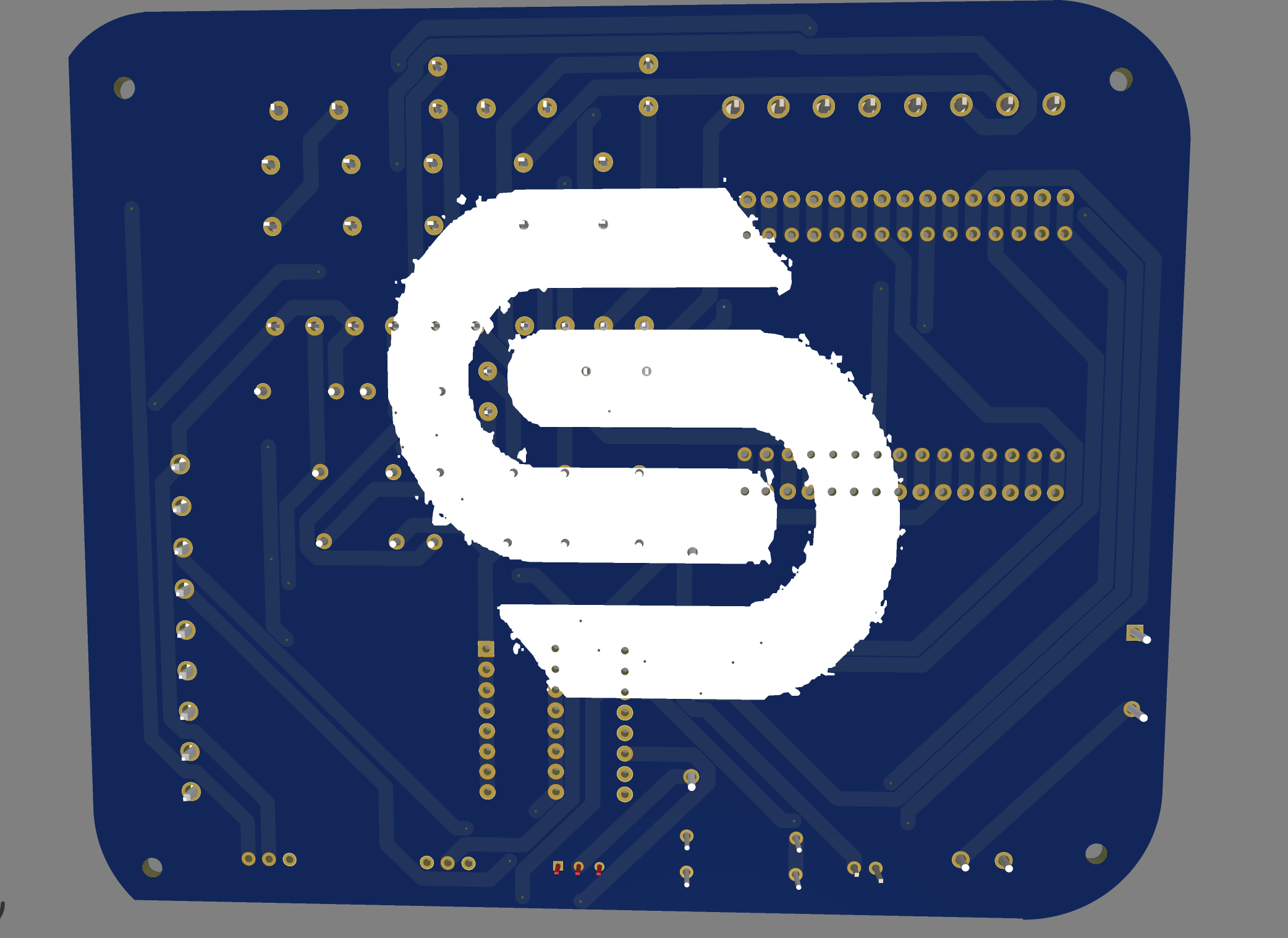
Wall-mounted touch control panel for home automation system featuring capacitive touch buttons, status LEDs, and relay control circuitry for appliance switching. Designed in EasyEDA with detailed schematic and routing diagrams for clear visualization.
Safety Design: Implemented proper isolation and creepage distances for safe 220V AC control on a 2-layer board.
Wearable PCB for hand gesture recognition
Compact wearable PCB for gesture-based presentation control featuring IMU for motion detection, capacitive touch for mode switching, and Bluetooth connectivity. This project represents my learning journey through multiple design iterations and improvements.
Have a circuit design in mind? Let's collaborate to create custom PCBs optimized for your specific requirements using EasyEDA and JLCPCB manufacturing.